Privacy statement: Your privacy is very important to Us. Our company promises not to disclose your personal information to any external company with out your explicit permission.
Model No.: YZPST-M1A080120L1
Brand: YZPST
Place Of Origin: China
VDSmax: 1200V
VGSmax: -10/+25V
VGSop: -5/+20V
ID Tc=25℃: 36A
ID Tc=100℃: 24A
ID(pulse): 80A
PD: 192W
TJ, TSTG: -55 to +150℃
Packaging: 1. Anti-electrostatic packaging 2. Carton box 3. braid
Productivity: 1000000000
Transportation: Ocean,Land,Express,Others,Air
Place of Origin: CHINA
Supply Ability: 100000000
Port: SHANGHAI
Payment Type: L/C,T/T,Paypal
Incoterm: CFR,FOB,CIF
Pulsed Power applications

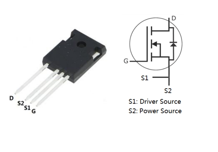
Part Number Package M1A080120 L1 TO-247-4
Maximum Ratings (TC=25℃ unless otherwise specified)
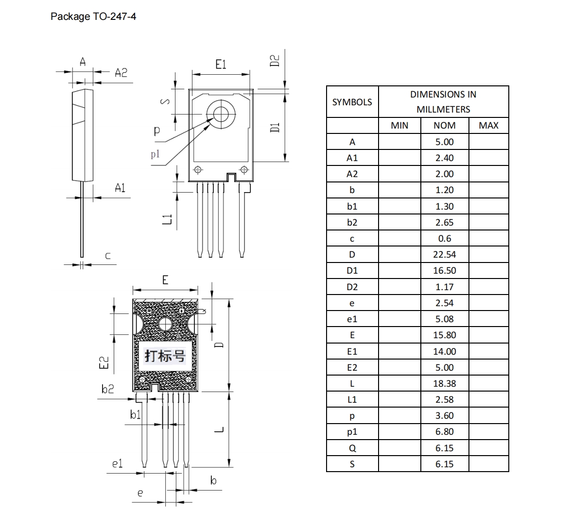
Electrical Characteristics (TC=25℃ unless otherwise specified) Reverse Diode Characteristics Package Dimensions Package TO-247-4
Symbol Parameter Value Unit Test Conditions Note VDSmax Drain-Source Voltage 1200 V VGS=0V, ID=100μA VGSmax Gate-Source Voltage -0.4 V Absolute maximum values VGSop Gate-Source Voltage -0.25 V Recommended operational values ID Continuous Drain Current 36 A VGS=20V, Tc=25℃ 24 VGS=20V, Tc=100℃ ID(pulse) Pulsed Drain Current 80 A Pulse width tp limited by TJmax PD Power Dissipation 192 W Tc=25℃, TJ=150℃ TJ, TSTG Operating Junction and Storage Temperature -55 to +150 ℃
Symbol Parameter Min. Typ. Max. Unit Test Conditions Note V(BR)DSS Drain-Source Breakdown Voltage 1200 / / V VGS=0V, ID=100μA VGS(th) Gate Threshold Voltage 2 2.4 4 V VDS=VGS, ID=5mA Fig. 11 / 1.8 / VDS=VGS, ID=5mA, TJ=150℃ IDSS Zero Gate Voltage Drain Current / 1 100 µA VDS=1200V, VGS=0V IGSS+ Gate-Source Leakage Current / 10 250 nA VDS=0V, VGS=25V IGSS- Gate-Source Leakage Current / 10 250 nA VDS=0V, VGS=-10V RDS(on) Drain-Source On-State Resistance / 80 98 mΩ VGS=20V, ID=20A Fig. / 140 / VGS=20V, ID=20A, TJ=150℃ 4,5,6 Ciss Input Capacitance / 1475 / VGS=0V Fig. Coss Output Capacitance / 94 / pF VDS=1000V 15,16 Crss Reverse Transfer Capacitance / 11 / f=1MHz Eoss Coss Stored Energy / 52 / µJ VAC=25mV EON Turn-On Switching Energy / 564 / µJ VDS=800V, VGS=-5V/20V EOFF Turn-Off Switching Energy / 260 / ID=20A, RG(ext)=2.5Ω, L=200μH td(on) Turn-On Delay Time / 9.3 / tr Rise Time / 9.5 / VDS=800V, VGS=-5V/20V, ID=20A RG(ext)=2.5Ω, RL=40Ω td(off) Turn-Off Delay Time / 18 / ns tf Fall Time / 7.6 / RG(int) Internal Gate Resistance / 3.1 / Ω f=1MHz, VAC=25mV QGS Gate to Source Charge / 24 / VDS=800V QGD Gate to Drain Charge / 15 / nC VGS=-5V/20V QG Total Gate Charge / 79 / ID=20A
Symbol Parameter Typ. Max. Unit Test Conditions Note VSD Diode Forward Voltage 3.6 / V VGS=-5V, ISD=10A Fig. 8,9,10 3.3 / VGS=-5V, ISD=10A, TJ=150℃ IS Continuous Diode Forward Current / 44 A TC=25℃ trr Reverse Recover Time 35 / ns Qrr Reverse Recovery Charge 91 / nC VR=800V, ISD=20A Irrm Peak Reverse Recovery Current 4.5 / A 
Product Categories : Semiconductor Plastic Package > Silicon Transistor


Privacy statement: Your privacy is very important to Us. Our company promises not to disclose your personal information to any external company with out your explicit permission.

Fill in more information so that we can get in touch with you faster
Privacy statement: Your privacy is very important to Us. Our company promises not to disclose your personal information to any external company with out your explicit permission.